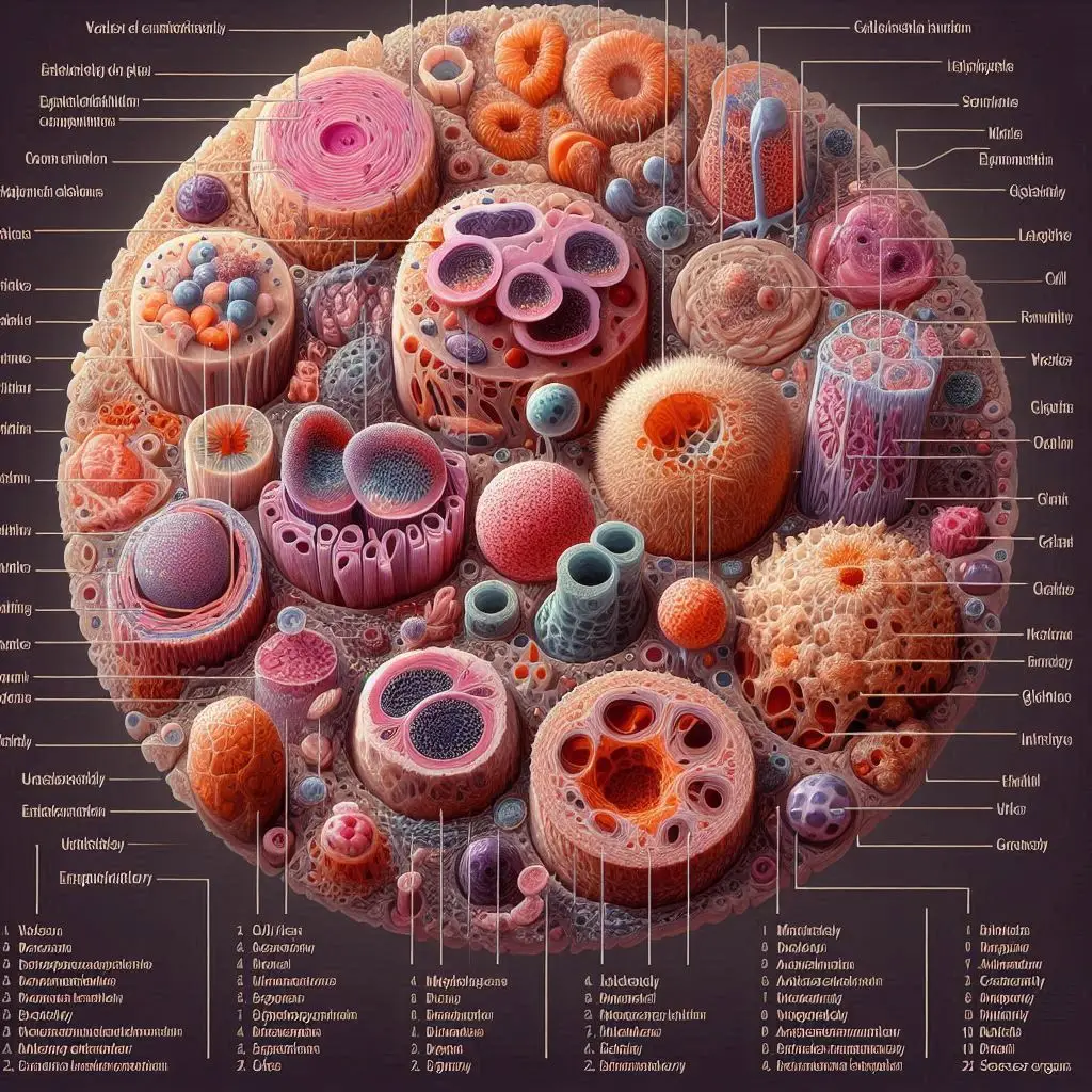
Electron Microscopes

Introduction to Electron Microscopes
These instruments are essential in many scientific disciplines, including biology, materials science, and nanotechnology. They provide detailed images that reveal the fine structure of cells, materials, and other small objects. Unlike optical microscopes that rely on visible light, electron microscopes use electrons, which have much shorter wavelengths. This property allows them to achieve much higher resolutions. By employing these particular techniques, researchers can delve into the microscopic world with unprecedented clarity.
How Electron Microscopes Work
At the core of an electron microscope is the electron beam generated by an electron gun. This beam is focused onto the specimen using electromagnetic lenses. When the electrons interact with the sample, they produce various signals that can be detected and converted into images.
Key Components of Electron Microscopes
1. Electron Gun
The source of electrons, usually made from tungsten.
2. Electromagnetic Lenses
These lenses focus the electron beam onto the specimen.
3. Sample Holder
Holds the specimen in place during imaging.
4. Image Viewing System
Converts signals from the specimen into a visible image.
For a detailed overview of these components, you can refer to Optical Mechanics.
Types of Electron Microscopes
There are primarily two types of electron microscopes: Transmission Electron Microscopes (TEM) and Scanning Electron Microscopes (SEM). Each type has unique features and applications.
Transmission Electron Microscope (TEM)
Overview: TEMs provide images by transmitting electrons through a thin specimen. They can achieve resolutions down to 0.1 nm.
Working Principle:
- The electron beam passes through the specimen.
- Interactions between electrons and atoms create an image based on variations in density.
Applications:
- Used extensively in biological research to study cell structures.
- Important for materials science to analyze crystal structures.
For more information about TEMs, visit VacCoat.
Scanning Electron Microscope (SEM)
Overview: SEMs scan a focused beam of electrons across a specimen’s surface to produce detailed three-dimensional images.
Working Principle:
- The electron beam interacts with the surface atoms.
- Secondary electrons emitted from the surface are detected to form an image.
Applications:
- Ideal for examining surface morphology and composition.
- Widely used in industrial applications for quality control.
For further details on SEMs, you can check out Wikipedia.
Advantages of Electron Microscopes
Electron microscopes offer several advantages over traditional optical microscopes:
- Higher Resolution: They can resolve structures at a much finer scale due to shorter wavelengths.
- Detailed Imaging: Provide comprehensive images that reveal both surface and internal features.
- Versatile Applications: Useful in various fields from biology to nanotechnology.
Limitations of Electron Microscopes
Despite their advantages, electron microscopes come with limitations:
- Sample Preparation: Specimens often require extensive preparation to be suitable for imaging.
- Vacuum Requirement: The operation requires a vacuum environment, which can complicate sample handling.
- Cost: They are generally more expensive than optical microscopes.
The Future of Electron Microscopy
The field of electron microscopy continues to evolve with advancements in technology. New techniques such as cryo-electron microscopy allow researchers to observe biological specimens in their native state without extensive preparation.
Conclusion
Thus these invaluable tools have transformed our understanding of the microscopic world. By utilizing beams of electrons instead of light, they provide unprecedented detail and clarity in imaging. As technology advances, we can expect even more innovative applications and improvements in this field.
For more pearls of Vets Wisdom:


Your article helped me a lot, is there any more related content? Thanks!